
Project Overview
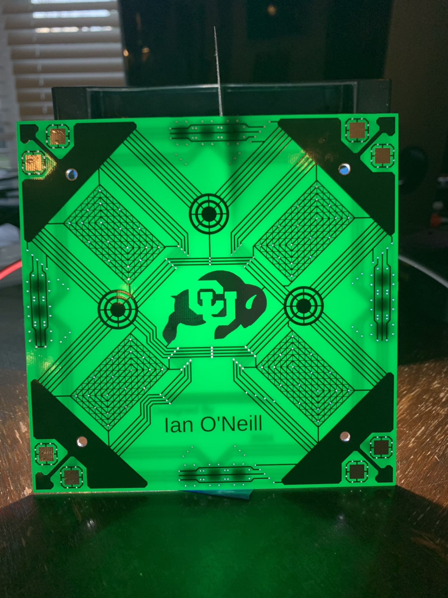
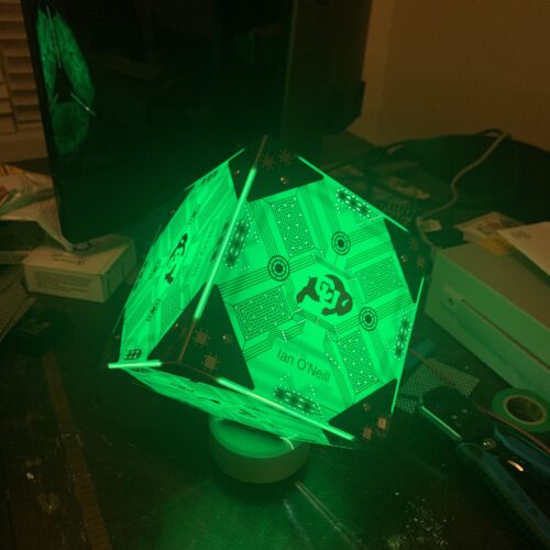
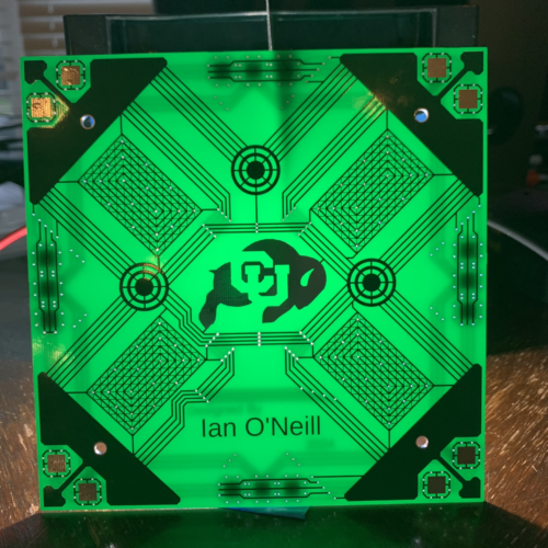
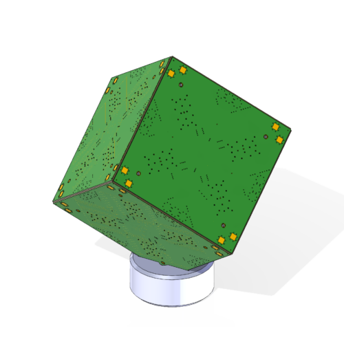
For this project, I endeavored on designing a cube shape lamp made out of PCBs (printed circuit boards). The final outcome is shown below:
The goal of this was to create an ambient light lamp designed according to a PCB aesthetic, something quite unique with a lot of potential.
Project Requirements
The following requirements and constraints are what I determined to be the key requirements of the PCB Lamp sorted into two categories: aesthetic and functional:
Aesthetic Requirements
- The lamp should be cube shaped
- The lamp’s construction material should be PCBs to conform to the PCB aesthetic
- While off, the lamp should be visually interesting
- While on, the lamp should show contrast and change appearance
- While on, the lamp should provide enough ambient lighting to have some vision in a dark room
Functional Requirements
- The lamp should be battery powered and able to recharge with a runtime of at least 2 hours
- The lamp should have variable brightness controlled by PWM
- The lamp should be operable with or without the base
- The lamp base should automatically begin charging once the lamp is attached
Project Inspiration
This year on my senior design team I chose to be the electromechanical engineer for my team and have been working closely with PCBs all year. In doing so, I wanted to try to incorporate them into more of my projects. During the brainstorming phase of the final project, I came up with two main ideas for what my project could be: an ambient light lamp or a clock whose walls were PCBs.
[Image of concept sketches]Eventually I settled on attempting the lamp after coming across a random image displaying the unique look which appears gives off a really unique glowing effect when backlit.
The Aesthetic: PCBs
I feel that this aesthetic is one of the few where the material drives the aesthetic, and not the other way around. Generally an aesthetic is not exclusive to any one material, however, when coming up with this idea, I wanted to be able to accentuate the key characteristics of a PCB. This was done by backlighting the PCBs in order to create a unique style of lamp.
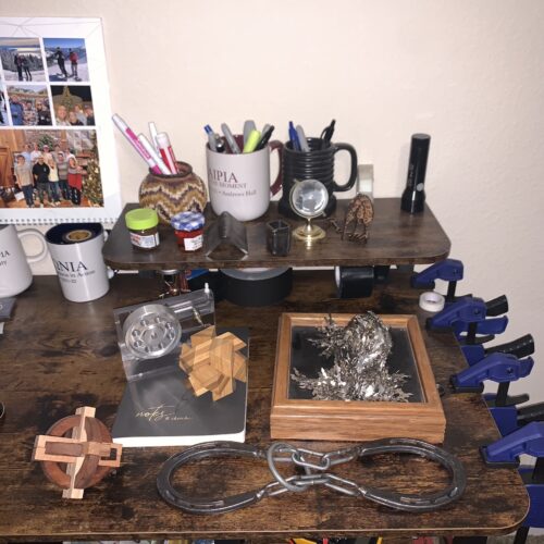
Additionally, I thought of this aesthetic due to the fact that I knew this would be a standout piece. Because PCBs are generally closed off from the world, they spark a lot of interest when people are actually able to see, feel, and interact with them. Art pieces which challenge the norm or follow unique styles will also spark this unique interest. On my desk in my room, I like to keep various trinkets that people can fiddle with, talk about, and be puzzled by. Notable items are a horseshoe puzzle and magnetic sculpture toy. These are often fun conversation starters and ways to pique new interest. This lamp would be a new fun addition to the collection by adding a visually striking piece.
The Glow Effect
All of the areas where copper remains within the PCB exist as silhouettes while the non-coppered areas are get to glow. Traditionally, PCBs are designed purely for functionality. Almost never will a final product expose the PCB, or the brains behind it. Generally they are kept safe in a box, out of sight for aesthetic purposes and protection purposes. I decided to go completely against this standard and utilize the PCB as my main construction material.
In order to test the glow effect, I found various PCBs and shown lights up behind them.
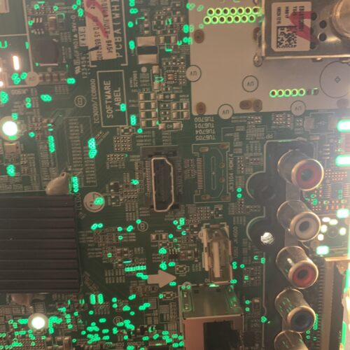
One notable shortcoming of existing PCBs is their lack of “glow.” This can be explained by the presence of a ground plane. In PCB design, standard practice is to create a ground plane on at least one layer. This means making the entire layer solid copper except for areas where you need clearance from the ground signal. This can be for routing vias, pads, or other signal tracks. In order to ensure effective glowing, I knew I would forego this standard and manually rout all of the ground signals. Ground planes are usually used to reduce noise, however, I was able to remove the ground plane without problems for the following two reasons. The first is that I do not need to keep a high level of signal integrity and noise reduction. The second is that on these PCBs, the GND track is only being used for power which is running in one consistent direction and no high speed changes. Commonly, signal integrity must be handled carefully when dealing with high switching speeds (in the megahertz) or sensitive analog signals (think antennas), and my project utilizes neither of those.
The First Look
When the shipment of PCBs arrived, the first thing I did was hold them up to the light to see how they looked
The initial results are great! As you can see, I did not follow standard PCB practice and did not utilize a ground plane. This would defeat the entire purpose of the project! Instead, I manually routed all tracks as they need to be for visual and functional effects. Given that the only functional requirements are for power to be routed from the pads in the corner to the pads on the bottom of the backside, this did not pose any issue.
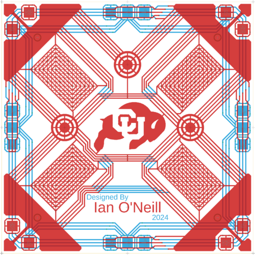
The glow effect is great, however, not quite what I was expecting. Referencing the image below, I thought I could utilize the top and bottom layers of the PCB to make it such that new patterns appeared when the lamp was turned on. One example is where it says “Designed by,” “Ian O’Neill,” and “2024” on alternating layers. In the final PCB, the “Designed by” and the “2024” are unreadable due to the light diffusion which occurs between the top and bottom layer meaning I have lost some detail. Fortunately, these were not crucial aspects for the appearance of the lamp.
The Components
This lamp design consisted of a few major components. The two which are exposed are the lamp base and the lamp panels which make up the lamp.
Internally, the design consists of 8 corner brackets and the LED to provide lighting
The Panels
The panels are where the artistic component of the project really shows. In order to create enough contrast to make the style pop, extra copper traces were added in, ones that have no function, in order to generate more texture on top while the lamp is on. Functionally, the PCBs are designed such that the cube can be placed down in any orientation and begin charging without being plugged in backwards.
The above images show the side by side comparison of the expected appearance to the actual appearance. All in all, the results turned out very well!
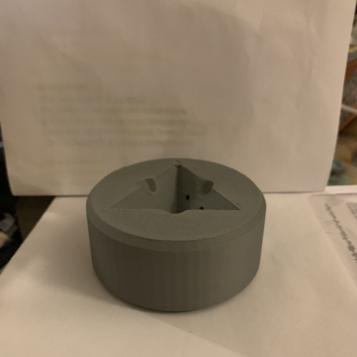
The Base
The base is a 3D printed component whose job is to keep the battery charged when in contact. Additionally, it keeps the lamp propped up at a different angle than if the lamp were sitting flat on a desk.
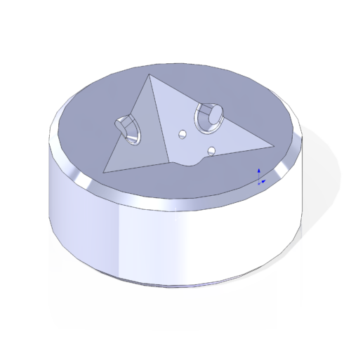
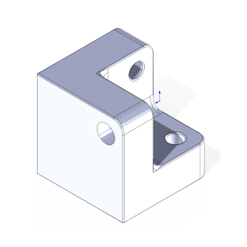
The Corner Brackets
These corner brackets are the main structural component of the lamp and are what hold the lamp in shape. They were constructed using a 3D printer with heat set inserts later added in order to be able to screw into the 3D printed components.
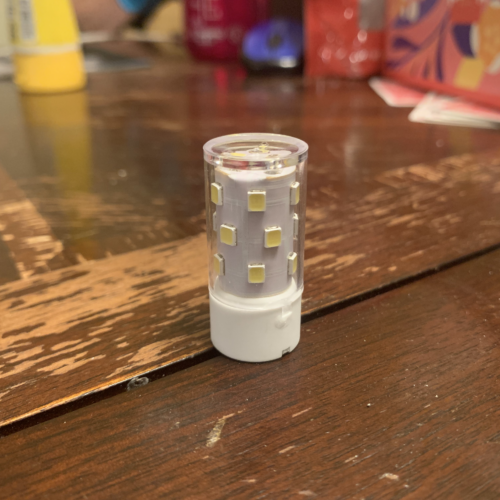
The LED
The LED chosen is one which consists of an array of LEDs around the side and on the top of the package. This allows for a wide led diffusion angle in order to properly light up all of the panels of the lamp. It additionally has internal drivers which accept a range of voltages from 10-20 volts, although it may go higher but I did not test it to failure. This flexibility helps to greatly simplify the electronics involved. Generally when running LEDs, a constant current driver is used, however, this is an additional step in the design which can add complexity. By using an LED with integrated drivers, it makes it very difficult to power the device incorrectly.
Conclusion
Overall, this project is a huge success! There is still work to do and improvements I would like to make which will be coming in the next post. Until then, I will continue to use this lamp for some ambient lighting. I would be curious to explore the effects silkscreens or different colored solder masks may have in the future! If you made it this far, thank you so much for reading and I hope you enjoyed it.
6 Comments. Leave new
[…] The What and Why [https://www.aesdes.org/2024/04/26/pcb-lamp-the-what-and-why/] […]
[…] Over the course of this semester and some of my previous post, I have been documenting the work done in order to design, manufacture, and assemble a lamp which utilizes PCBs as the main building material. More details can be seen in my previous post: https://www.aesdes.org/2024/04/26/pcb-lamp-the-what-and-why/ […]
This just might be the coolest thing I have ever seen! I love how you did the base holder interface with the design, extremely smart! It was also amazing hearing about how you tested the possibility of the project by shining light through other boards and getting to learn about the PCB layers was great. All in all amazing work!
Hi Colton, thanks for all the enthusiasm! It was truly a really fun and cool project and it came out even better than I expected! I’ll be sure to have it out at expo, so if you are attending, be sure to stop by!
Definitely an awesome utility to have the cube charge regardless of orientation. While I acknowledge that the aim was to emulate PCB boards, would you have considered having other colored cubes?
Hi Vincent, I did consider other board colors, however, I settled on green in order to leave the PCBs pronounced. Additionally, I may not have made it clear, but these panels are made out of real PCBs, not just emulating them. Other colors would work as well as I did test one which was purple and it showed similar effect just with a different color. If the goal is to have a more passive PCB aesthetic, a color such as black or white may be more appropriate.